The “all-silicon optoelectronic chip” project led by JI Professor Yaping Dan and jointly participated by another JI postdoctorate Huimin Wen serves to solve the bottleneck problem encountered during the constant downscaling of the feature size of the integrated circuit (IC). As the feature size of the IC is reduced to deep nanometer scale, traditional
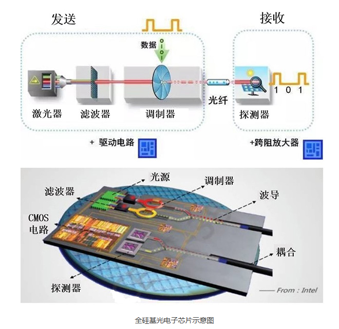
metal interconnect has become the main bottleneck restricting the development of IC due to RC delay and heat dissipation. The use of light on silicon wafers to replace traditional copper wires as information transmission media can greatly increase the transmission speed between chips. Therefore, the combination of ICs and photonics, constituting a CMOS-integrated all-silicon optoelectronic chip, is the only way to break the bottleneck. It can fully utilize the advantages of high integration, low cost of ICs and high bandwidth, ultra-fast transmissionrate of photonics.

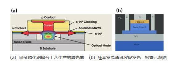
The main issue of the silicon-based optoelectronic technology is the integration of light sources with the IC. Silicon is widely known as an indirect bandgap semiconductor that cannot emit light at communication wavelength. At present, the mainstream of the silicon optoelectronics is the hybrid integration. III-V semiconductor lasers (InP, etc.) are applied as the light sources on silicon chip by discrete mounting (Lightspeed, Luxtera, etc.) or wafer bonding processing (Intel, etc.).
The low integration density and high cost of the circuit greatly limit the development of silicon-based optoelectronic technology.

Earlier research by Professor Yaping Dan’s group successfully generated room temperature silicon light-emitting diode (LED) at communication wavelength by ion implanting rare earth element Er into silicon and performing deep cooling annealing process. The room temperature quantum efficiency reached 14 %. Dr. Xingyan Zhao’s research project will forge ahead the process and integrate the silicon LED light source with CMOS circuits, modulators, photodetectors and optical
waveguides on the same chip to achieve the all-silicon optoelectronic chip. The all-silicon optoelectronic chip will enhance the integration density and lower the cost significantly, which is expected to be a milestone in the development of the communication technology.
The Postdoctoral Innovative Talent Support Program is a State-level plan established by China’s Ministry of Human Resources and Social Security and the National Postdoctoral Management Committee with the purpose of cultivating high-level innovative young talents with potential of penetrating into the forefront of science and technology on the global level. A total of 400 young postdoctorates were selected this year with engagement of pursuing postdoctoral research. The selected candidate is entitled with a grant of RMB600,000 covering a period of two years.