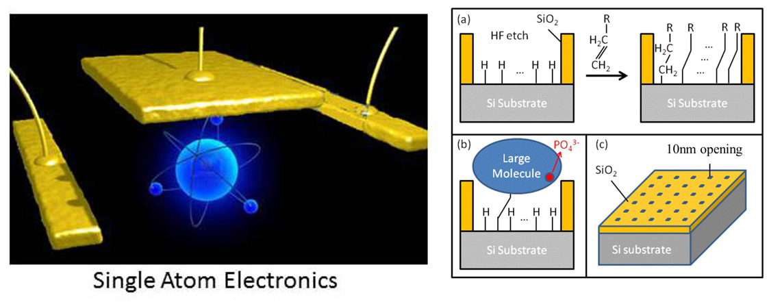
Single atom transistor schematic (left) and self-assembled molecular monolayer doping for single atom control (right)
单原子晶体管示意图(左)和自限制的单分子自组装(右)
Related Publications:/发表的相关论文
1. Deep level transient spectroscopic investigation of phosphorus-doped silicon by
self-assembled molecular monolayers
Xuejiao Gao#, Bin Guan#, Abdelmadjid Mesli, Kaixiang Chen and Yaping Dan*
Nature Communications 9 (2018) 118
2. Atomically thin delta-doping of self-assembled molecular monolayers by flash lamp annealing for Si-based deep UV photodiodes
Shannan Chang, Jiajing He, Slawomir Prucnal, Jieyin Zhang, Jianjun Zhang, Shenqiang Zhou, Manfred Helm, Yaping Dan*
ACS Applied Materials and Interfaces 14 (2022) 30000-30006. (Journal Cover)
3. Wafer-scale deep UV Si photodiodes based on ultra-shallow junction
Shuwen Guo, Shannan Chang, Zhengfang Fan, Zhijuan Su, Yueyang Jia, Jian Xu, Fengdan Wang, Liying Wu, Slawomir Prucnal, Shengqiang Zhou, Xiaolong Zhao, Rui Yang, Yongning He, and Yaping Dan*
IEEE Electron Device Letters 45 (2024) 944-947

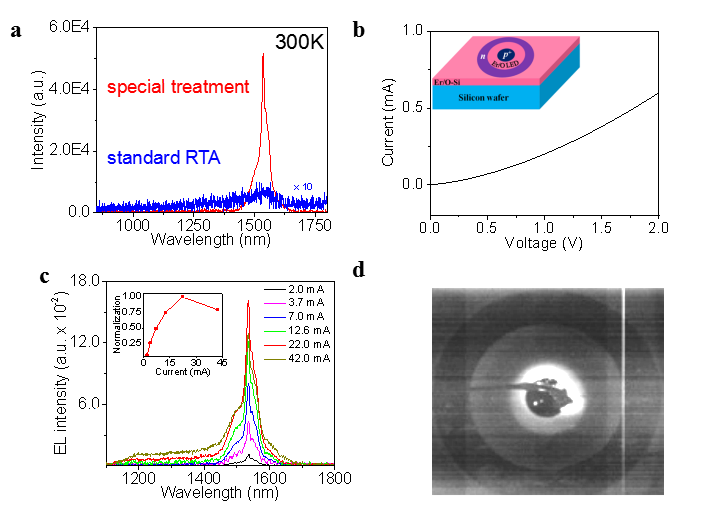
1. Efficient Er/O-doped Silicon Light-emitting Diodes at Communication Wavelength by Deep Cooling
Huimin Wen#, Jiajing He#, Jing Hong#, Shenbao Jin, Zhenming Xu, Hong Zhu, Jingquan Liu, Gang Sha, Fangyu Yue* and Yaping Dan*
Advanced Optical Materials 18 (2020) 2000720
2. Efficient Er/O Doped Silicon Photodiodes at Communication Wavelengths by Deep Cooling
Xingyan Zhao, Kaiman Lin, Sai Gao, Huayou Liu, Jiajing He, Xiaoming Wang, Huimin Wen, Yaping Dan*
Advanced Materials Technologies 6 (2021) 2100137
3. Analytical impact excitation of Er/O/B co-doped Si light emitting diodes
Xiaoming Wang, Jiajing He, Ao Wang, Kun Zhang, Yufei Sheng, Weida Hu, Chaoyuan Jin, Hua Bao, Yaping Dan*
Physical Review Letters 2024 (accepted) Highlighted as the Editor's Suggestion

Related Publications/发表的相关论文
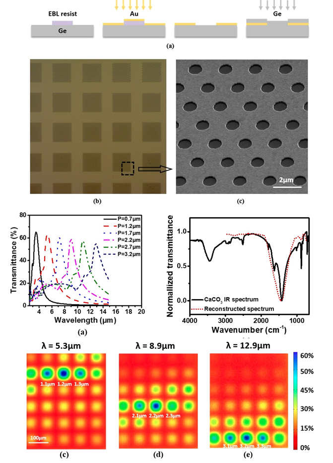
1. Mid-infrared plasmonic multispectral filters
Ang Wang and Yaping Dan*
Scientific Reports 8 (2018) 11257
2. Plasmonic micropipe spectral filters in mid-infrared
Jian Xu#, Ang Wang# and Yaping Dan*
Optics Letters 44 (2019) 4479-4482
3. High-performance plasmonic mid-infrared bandpass filters by inverse design
Jiarui Zhang, Zeji Chen, Zhijuan Su* and Yaping Dan*
Nanotechnology 35 (2024) 175202
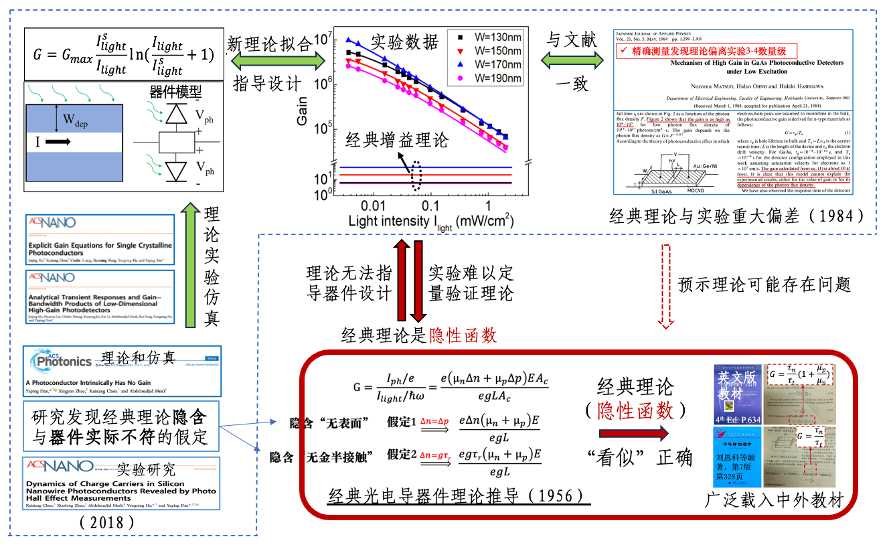
Photoconductor devices are the simplest photodetectors in terms of structure (no need for doping, etc.), but they have a huge quantum efficiency gain (up to 10 billion times), which is far superior to that of conventional diodes, bipolar transistors, and avalanche diodes, and thus they have the potential to develop high-sensitivity photodetectors, especially for defense-specific semiconductor devices. However, such devices have not been widely used in practical applications, one of the reasons being the lack of an explicit theory that can guide the design of the devices, since the existing classical theory is not only a hidden function but even fundamentally flawed. My research team found that there are two premise assumptions in the classical theory that are inconsistent with the actual devices (ACS Photonics 2018), and based on a large number of experimental studies (ACS Nano 2018, 2020, 2021), we have established a complete theory of the new explicit photoconductive devices, which provides an important theoretical basis for the design and optimization of the comprehensive performance of the photoconductive devices, and is expected to rewrite some chapters of classic semiconductor physics textbooks and promote the wide application of high-gain photoconductive devices.

Related Publications/发表的相关论文
1. Analytical Transient Responses and Gain-Bandwidth-Products of Low-Dimensional High Gain Photodetectors
Jiajing He, Huayou Liu, Chulin Huang, Yueyang Jia, Kai Li, Abdelmadjid Mesli, Rui Yang, Yongning He, Yaping Dan*
ACS Nano 15 (2021) 20242-20252 pdf
2. Explicit Gain Equations for Single Crystalline Photoconductors
Jiajing He#, Kaixiang Chen#, Chulin Huang, Xiaoming Wang, Yongning He, Yaping Dan*
ACS Nano 14 (2020) 3405-3413 pdf
3. A photoconductor intrinsically has no gain
Yaping Dan*, Xingyan Zhao, Kaixiang Chen and Abdelmajid Mesli
ACS Photonics 5 (2018) 4111–4116 pdf
4. Dynamics of charge carriers in silicon nanowire photoconductors revealed by photo Hall effect measurements
Kaixiang Chen, Xiaolong Zhao, Abdelmadjid Mesli, Yongning He* and Yaping Dan*
ACS Nano 12 (2018) 3436-3441 pdf
